
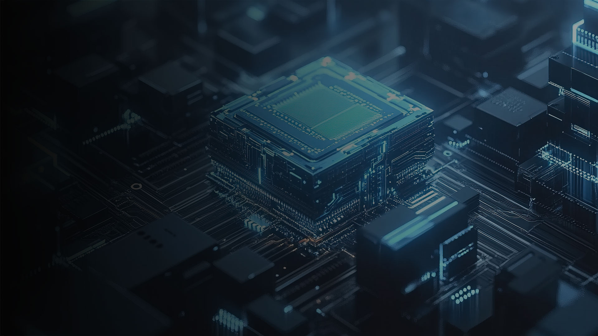
Wafer Cleaning
In the front - end semiconductor process, metal ions, polishing particles (such as cerium oxide), and organic substances remaining on the wafer surface need to be thoroughly removed. Ultrasonic waves strip off contaminants through the high - frequency cavitation effect (20kHz - 1MHz). After cleaning, the cleanliness of the wafer surface can reach ≤5 particles (≥0.3μm)/cm², meeting the requirements of subsequent processes such as lithography and deposition. For example, the cleaning of polysilicon wafers requires a multi - stage process combining deionized water and alkaline solution, and uniform cleaning is achieved through automated operation by a robotic arm.
Photoresist Residue Removal
The photoresist and chemical substances remaining after lithography will affect the subsequent etching accuracy. The ultrasonic cleaning machine, in combination with an ammonia/hydrogen peroxide mixture (SC - 1) or ozone water, can decompose and remove nanoscale colloidal residues while avoiding damage to the micro - structure on the wafer surface. A certain case shows that after using 130kHz high - frequency ultrasonic waves, the photoresist removal efficiency is increased by 40%.
Packaging and Testing Phases
Solder particles and grease generated during the chip packaging process need to be thoroughly cleaned. The ultrasonic cleaning machine penetrates into the gaps between BGA solder balls through the cavitation effect to remove contaminants and ensure packaging reliability. Cleaning before testing can reduce signal interference and improve the yield rate. The actual measurement of VGT equipment shows that the qualified rate of the electrical performance of the packaged chip is increased from 92% to 99.5%.
地址:
Room 801, 8th Floor, Building 1, No. 90, Aigehao Road, Weitang Town, Xiangcheng District, Suzhou City联系电话:
15250467891邮箱:
jiwenchang@spring-sz.comCopyright © 2025 润斯普瑞超声科技(苏州)有限公司版权所有 苏ICP备2021041029号-1
欢迎致电:
15250467891
打开微信扫一扫
联系我们


